- 您现在的位置:买卖IC网 > Sheet目录311 > AS3665-ZWLT (ams)IC LED DRIVER SMARTLIGHT 25WLCSP
AS3665
Datasheet, Confidential - P i n o u t
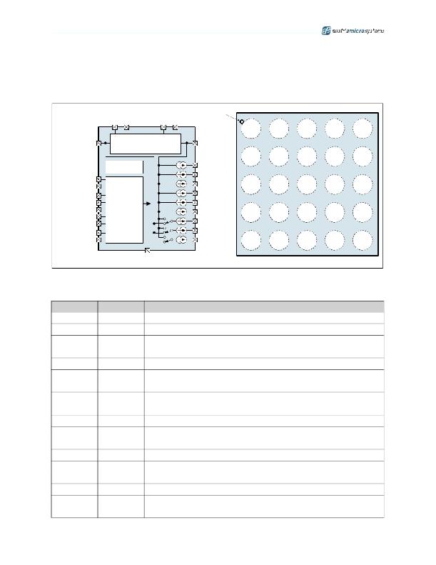
4 Pinout
Pin Assignment
Figure 2. Pin Assignments WL-CSP-25 (2.610x2.675mm) 0.5mm pitch (Top View)
3
4
.
3
4
"
!" % #
4
4
5
,
1
0
2. (
.
2
2. (
.
.
3
.,
7
2 2
.
.
/
%
"
,
6, 6
(7!5
! (8 9 !:;!
5 :
2 2 .
7 .,
! !"# $ %
& "%
## "
"# '
( #
) "%
*"% " + # "
.
,
,
,
-
/
0
1
2
3
,
,
,
-
,
(7!5 5 :
6, 6 ! (8 9 !:;!
5
,
AS3665
AS3665
Pin Description
Table 1. Pin Description for AS3665
Digital input - I C address select; the value of the resistor R ADDR defines the actual
I C address used
Pin Number
A1
A2
A3
A4
A5
B1
B2
B3
B4
B5
C1
C2
C3
C4
C5
D1
D2
Pin Name
C2-
C1-
GND
LED9
LED8
VBAT
C2+
ADDR
C 2V5
LED7
VCP
C1+
LED3
TRIG
GPO
LED2
LED1
Description
Charge Pump flying capacitor 2 - make a short connection to capacitor C FLY2
Charge Pump flying capacitor 1 - make a short connection to capacitor C FLY1
Ground supply input pin
LED9 output - current source from VCP or VBAT
LED8 output - current source from VCP or VBAT
Positive supply input pin
Charge Pump flying capacitor 2 - make a short connection to capacitor C FLY2
2
2
Internal supply - connect a 1μF ceramic capacitor between C 2V5 and GND
LED7 output - current source from VCP or VBAT
Charge Pump output - make a short connection to capacitor C VCPOUT
Charge Pump flying capacitor 1 - make a short connection to capacitor C FLY1
LED3 output - current source from VCP
Digital open drain input/output - used to synchronize across several AS3665
Digital open drain input/output - General purpose output and ADC input
LED2 output - current source from VCP
LED1 output - current source from VCP
www.austriamicrosystems.com
Revision 1.0.2
2 - 77
发布紧急采购,3分钟左右您将得到回复。
相关PDF资料
AS3685B-T
IC DVR PHOTOFLASH 1A 10-DFN
AS3685C-T
IC DVR PHOTOFLASH 1A 10-DFN
AS3691B-ZMFT
IC LED DVR 400MA RGB/WHT 64-MLF
AS3691B-ZTSP
IC LED DVR 400MA RGB/WH 20ETSSOP
AS3693A-ZQFT
IC LED DVR 16CH W/PWM 48-QFN
AS3693B-ZTQT
IC LED CTLR 16-CH W/PWM 64-TQFP
AS3693B-ZTQW
IC LED CTLR 16-CH W/PWM 64EPTQFP
AS5040 PB
BOARD PROGRAM AS5040
相关代理商/技术参数
AS3665-ZWLT-500
功能描述:IC SMARTLIGHT DRIVER 25WLCSP RoHS:是 类别:集成电路 (IC) >> PMIC - LED 驱动器 系列:- 特色产品:LM3445 TRIAC Dimmable LED Driver 标准包装:55 系列:PowerWise® 恒定电流:是 恒定电压:- 拓扑:PWM,降压(降压) 输出数:1 内部驱动器:无 类型 - 主要:- 类型 - 次要:高亮度 LED(HBLED) 频率:30kHz ~ 1MHz 电源电压:8 V ~ 12 V 输出电压:- 安装类型:表面贴装 封装/外壳:14-SOIC(0.154",3.90mm 宽) 供应商设备封装:14-SOICN 包装:管件 工作温度:-40°C ~ 125°C 产品目录页面:1285 (CN2011-ZH PDF) 其它名称:LM3445M
AS3668
制造商:AMSCO 制造商全称:austriamicrosystems AG 功能描述:4 Channel Breathlight Controller
AS3668 EB
制造商:ams 功能描述:BOARD EVAL FOR AS3668
AS3668_07
制造商:AMSCO 制造商全称:austriamicrosystems AG 功能描述:4 Channel Breathlight Controller
AS3668-BQFT
功能描述:IC LED DRVR BACKLIGHT 12-WLCSP RoHS:是 类别:集成电路 (IC) >> PMIC - LED 驱动器 系列:- 特色产品:LM3445 TRIAC Dimmable LED Driver 标准包装:55 系列:PowerWise® 恒定电流:是 恒定电压:- 拓扑:PWM,降压(降压) 输出数:1 内部驱动器:无 类型 - 主要:- 类型 - 次要:高亮度 LED(HBLED) 频率:30kHz ~ 1MHz 电源电压:8 V ~ 12 V 输出电压:- 安装类型:表面贴装 封装/外壳:14-SOIC(0.154",3.90mm 宽) 供应商设备封装:14-SOICN 包装:管件 工作温度:-40°C ~ 125°C 产品目录页面:1285 (CN2011-ZH PDF) 其它名称:LM3445M
AS3668-BWLT
制造商:ams 功能描述:IC LED DRVR BACKLIGHT 12-WLCSP
AS3668-EB
制造商:ams 功能描述:Evaluation Board
AS366R5FLF
制造商:TT Electronics / IRC 功能描述:AS366R5FLF
